
Readout Electronics
Overview
The signal of an imaging sensor must be amplified without adding considerable noise. Furthermore, the electronics must be immune to external noise sources. For the AMBER instrument, we use a specialized clocking scheme to read multiple sub-images. With LINC-NIRVANA, we read two quadrants of the imaging sensor independently at different frame rates. This requires a high flexibility in creating unconventional readout modes. The readout electronics we developed meet all these requirements. They are optimized to operate on HAWAII-1 infrared imaging sensors.


The main part of the electronics boards is kept at ambient temperature in a metallic block outside the dewar. The metallic block acts as housing, heat sink and electrical shield. The boards inside are optimally arranged to avoid electromagnetic interference. Only the fanout board, which carries the imaging sensor, is inside the dewar at cryogenic temperature. The functionality of all the boards is described below.
Sequencer
The sequencer generates the clock patterns necessary for reading and sampling the imaging sensor. It can be configured via an Ethernet socket command server. It also generates a header containing information about image format, read mode etc.
Features
- 10 MHz system clock => 100 ns clock signal resolution
- 1M x 64 bit SRAM memory for readout pattern programs => 1M instructions
- 32 signals for clocking the imaging sensor
- 8 signals for ADC control
- 128 byte header information for each output frame
Hardware
The sequencer is a hybrid design consisting of two stacked PC104-modules:
- a Diamond Systems Helios HLV800-256DV single board computer
This is a fully PC-compatible x86-architecture running Debian/GNU Linux, equipped with a solidstate-drive, USB- and Ethernet controller. The module runs a command server based on Ethernet socket communication. The setup of the readout electronics is configured by communicating with the command server.
- a loop processor board
A Xilinx Spartan-3 FPGA hosts a loop processor with a small instructions set. The design includes an ISA-interface, SRAM-memory and differential line drivers. This board generates in real-time the clock signals for the imaging sensor readout.


Low Level Software
The loop processor works with a set of sixteen commands. The machine code execution produces one state of clock signals/ADC controls with every system clock tick. The sequencer hardware provides a flexible structure for repeating patterns like frames, lines, or pixels. Each state of the output signals is defined by software. Repeating patterns are put into loops. Loops can be nested to arbitrary levels only limited by the hardware resources of the FPGA. The device provides three groups of generated signals. One set is routed to the ADC board to control analog to digital conversion. Another set of signals are the clocks for driving the imaging sensor. The third set is connected to the pixel data bus to insert header information into the image data output stream.
High Level Software
The program code of a basic readout sequence resides in a program file. There are different ways to modify the readout (e.g. to change exposure time, region of interest, etc.). For example, one can communicate with the command server. One can also edit the program file itself. After receiving a command the command server changes the corresponding parameters and , if necessary, starts the compilation of the program code. The low level machine code is downloaded via the ISA-bus to the SRAM memory. The processing of the code is started by writing to the control register.
Clock Driver
The digital clock signals comming from the sequencer have to be boosted before they can drive the imaging sensor on the fanout board. The clock driver board receives the signals from the nearby sequencer board and drives twisted pair lines leading to the distant fanout board. There are up to 32 clock lines, which is enough to control all four quadrants of a HAWAII-1 imaging sensor independently.
If the cable length is longer than a few decimeters, the output impedance of the line driver must be matched to the line impedance at the near end. We do not use a termination at the far end of the line, because this would half the voltage and produce heat. However, this means that there are reflexions running back the line to be absorbed in the output impedance of the line driver. It is important that there are no discontinuities in the line impedance to be seen by the reflecting signal on its way back to the line driver. As long as these conditions are met, the cable can be up to several meters in length.


Fanout Board
The fanout board carries the imaging sensor in a socket and supplies it electrically with clock signals and voltages. It is operated at cryogenic temperature inside the dewar.
The video output of the imaging sensor will be too weak to be transmited to the outside if the cable length exceeds a few decimeters. Therefore, active amplification stages are placed onto the fanout board. Operational amplifiers with FET inputs are used to pre-amplify the video signals and to drive 50 Ohms transmission lines in differential mode. Thus, the cable can be up to several meters in length.


Video Amplifier
The video signals coming from the fanout board have to be processed before being converted into a digital data stream. The video amplifier board combines multiple functions of analog signal processing.
DC voltage generation
All voltages referring to the analog part of the fanout board are generated on the video amplifier board. Thus it is guaranteed that they refer to the same ground like the video signals do. There are: analog power, reset voltage, bias gate voltage, asymmetrical supply for cryogenic pre-amps and reference voltages for cryogenic pre-amps. All of these voltages are understood as signals of low noise, low impedance and constant voltage. The voltage sources are capable of using high-bandwidth currents to drive rapidly changing loads.


Basic signal processing
Each video input signal is shifted to an appropriate DC level and amplified to fit into the voltage range of the ADCs. Along with the filtering described below, the analog signal chain is designed to add as less noise as possible to the signal.
A low noise design requires that all stages occur in proper succession. For example stages which attenuate certain frequencies of the spectrum are placed at the end of the signal chain. For any noise which may be introduced along the singal chain this frequencies will be attenuated, too.
The division of the overall gain to the single amplifier stages is also important for a low-noise design. If the major amplification is at the input stage, the noise which may be introduced along the singal chain will be ampflified minimally. The input stage is the pre-amplifier on the fanout board. The gain of this stage is limited by the constraints resulting from the cryogenic operating temperature. The remaining amplification is taken over by the next stage of the video amplifier board. The gain of all further stages amounts to just a little more than one.
Analog filtering
A moving average filter is used in each video channel to reduce noise in the signal. The output of the filter is a continuous signal that is proportional to the average of the input during the past 100 ns. This time period matches the sampling period of the analog to digital conversion. Input signals which are older than 100 ns must not affect the current output signal (finite impulse response). The filter can mathematically be described as an integrator:
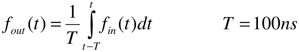


The step response and the frequency response of an ideal moving average filter are shown in the plots above. The practical implementation is a purely analog approximation of the filter characteristic. Series resonant circuits placed along a ladder of resistors create the first three zeros at 10 MHz, 20 MHz and 30 MHz. Two capacitors in between deskew the phase and attenuate the signal toward higher frequencies.


The quality factors Q1, Q2, Q3 of the three resonant cricuits and the two capacitors C1, C2 give five parameters to be adjusted to get the best matching filter characteristic. The behaviour of all other analog stages is factored in for the optimization process of the parameters. Thus, the influence of the other stages on the frequency response is compensated. As a result, the entire analog signal chain, from the imaging sensor output to the ADC input, complies with the desired moving average filter characteristic.
This analog filter is part of a filtering method which is continued on the digital side.
ADC (Analog Digital Converter)
The ADC board converts the analog video signals to digital samples, selects a subset of samples and calculates their average to get a pixel value.
The ADC board has four channels. The differential analog signals coming from the video amplifier board are sampled with 10 MHz and 14-bit resolution. Each channel has a Logic Cell Array (LCA), which adds up a variable number of samples and averages the sum to a 16-bit value. The generation of one resulting pixel value looks like:
- the sequencer produces the clock signals, which lead to addressing one pixel on the imaging sensor.
- the analog outputs of the imaging sensor are conditioned by the cold amplifiers on the fanout board
- the analog output of the fanout board is preprocessed on the video amplifier board.
- the differential analog output of the video amplifier is the input to the ADC.
- the sequencer controls the LCAs on the ADC board to add up a defined set of samples.
- the output of the LCAs is a 16-bit average value of the set of samples.
- the LCAs consecutively put their output on the 16-bit bus to the serial link transmitter.
- the serial link transmitter serializes (special protocol) the 16-bit value.
- a fibre optical transmitter puts out the serialized pixel value.
- the next pixel is addressed.
The concept of sub pixel sampling
The moving average filter bandwidth is matched to the ADC sampling speed. By simply adding individual ADC samples, the resulting bandwidth B is inversely proportional to the number of samples, multiplied by T:
B = k/(number of samples * T) with k ca. 1.05
After a pixel has been addressed, it takes some time for the analog signal to settle. When the signal is stable, it is sampled several times by the ADC (see figure below). This so called sub pixel sampling has several advantages:
- Noise can be reduced by averaging the samples taken within one pixel.
- Since the sample rate is constant, the analog signal acquisition is optimally adapted to the ADC at any pixel rate.
- The effective signal bandwidth is adapted to the pixel clock frequency by simply changing the number of samples.


Slowing down the pixel clock (frame rate) offers the opportiunity to average over a higher number of samples. Doubling the number of samples results in reducing the noise by a factor of 1/sqrt(2).