Implementation
Systematic studies were carried out by our group to establish a method to achieve best trade-offs between quantum efficiency, ultra-fast response times and device lifetime. Reproducible control over the concentration of ionized arsenic antisites (AsGa+), which act as electron ultrafast trapping centers in GaAs, is crucial to achieve these goals.

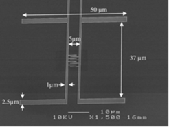


The photomixer metallization consists of small-area Ti/Au Metal-Semiconductor-Metal (MSM) structures feeding planar broad-band or resonant antennas. The metallization is patterned by standard electron-beam and optical lithography techniques. The external dc bias is applied to the MSM electrodes by electrically contacting the photomixer through bond pads. The optical coupling to the photomixer active area is realized by a single-mode fiber optic, positioned with submicron accuracy. Once the optimal illumination position has been achieved, the fiber is fixed to the photomixer. The (butt-coupled) photomixer and collimating lens are assembled in a compact housing, the assembly includes a fiber bend protection and a fiber patch with connector for the optical input.
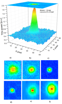
A chip containing the photomixer and the antenna and is mounted on a high resistivity silicon substrate lens, which (i) collimates the radiation, (ii) prevents the signal from being radiated backwards to the fiber optic which illuminates the device, (iv) suppresses surface modes and (v) provides a high beam directivity. In order to minimize aberration, the maximum of the antenna pattern is aligned with the optical axis of the silicon lens.